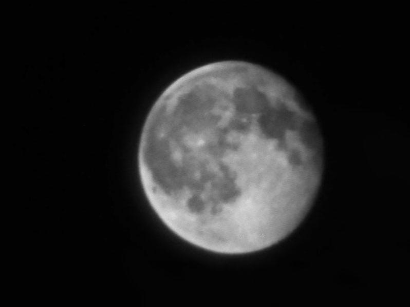
The picture of the Moon in the banner might not look all that spectacular, but it is absolutely astounding from a technical perspective. What makes it so unique is that it was taken via a telescope using a completely flat lens. This type of lens, called a metalens, has been around for a while, but a team of researchers from Pennsylvania State University (PSU) recently made the largest one ever. At eight cm in diameter, it was large enough to use in an actual telescope – and produce the above picture of the Moon, however, blurred it might be.
Metalenses have been produced before, but typically only on a millimeter scale. They utilize nanostructures etched into the surface of the lens itself, forcing the light that passes through them to a central focal point, much as the curved surface of a typical lens used in optics does. Part of the reason other metalenses have been relatively small in scale so far is the difficulty of creating those nanostructures on a larger lens structure.
For this, the team at PSU turned to an alternative manufacturing process – deep ultraviolet (DUV) photolithography, a process typically used to create high-speed computer chips. Compared to the typical metalens creation process of electron beam lithography, DUV has several advantages.
Credit – TEDx Talks YouTube Channel
First, it is repeatable at high speed. The team, led by Dr. Xingjie Ni, did what all good problem solvers do. They took a large problem – in this case, how to cover the surface of a 4 cm circle with nanostructured antennas – and broke it down into manageable chunks. Those chunks turned out to be 22 mm x 22 mm regions of the plate, and they then patterned the necessary antenna structures onto the lens using a DUV system at Cornell.
A second advantage is DUV is capable of consistently producing small details. This is especially true when it’s used to create transistors on a computer chip, but in this case, the nanostructured antennas could be produced with the same level of precision.
That isn’t to say the entire research process was as simple as running a new system to create a larger version of a known technology. The researchers had to significantly shrink the file size used to direct the DUV machine on how to operate. They did so by using data approximations and other file compression techniques.

Credit – Jeff Xu / Penn State
Even with all that effort, challenges remain – the most notable being chromatic aberration. Chromatic aberration occurs when different colors of light are bent by the nanostructured antennas differently. This creates different focal points for different colors of light, causing them to blur if collected in the same image. But Dr. Ni and his graduate students are working hard on designing a new and improved system that could eliminate the chromatic aberration problem and other optical issues caused by the flat surface.
However, astronomy isn’t the only practical application for these larger metalenses. Despite their ubiquity, the lenses of a cell phone’s camera are still curved, which takes up valuable space in its design. Typically, you can see a protuberance near the camera lens on the slimmest cell phone models. With a true metalens that works as intended, those issues could be eliminated, leading to an extensive install base if cell phone manufacturers become interested. Both amateur and professional astronomers would probably get some much better pictures of the Moon out of the deal as well.
Learn More:
PSU – Flat, pancake-sized metalens images lunar surface in an engineering first
Zhang et al – High-Efficiency, 80 mm Aperture Metalens Telescope
UT – Christiaan Huygens’ Telescope Lenses Tell Us He Was Nearsighted
UT – What are Telescopes?
Lead Image:
Image of the moon captured with a telescope utilizing the new, larger metalens.
Credit – Xingjie Ni

